Tuesday, July 8, 2014

Creating a RFID Reader From Scratch Part 2

ASK RFID Reader (for ISO11785)

The ASK reader that I implemented in my solution looked like this after drawing in all the components in Eagle:
The overall system can be split into two, the transmitter part, and the receiver part. The top-right most part of the circuit is the transmitter.

Transmitter 

The transmitter is a simple current amplifier, where the transistors Q1 and Q3 will alternately pull the antenna voltage high and low depending on the "control" signal in to the amplifier, thus forcing a high current through the antenna. The important thing to note is that this circuit does not generate any frequency signal on itself, it requires a source that produces the correct frequency, the carrier frequency in this case. For the original implementation from the Microchip application note this circuit was tunes to receive a 125 kHz signal, to generate the correct carrier frequency for 125 kHz RFID tags. In my implementation I had to change this to 134.2 kHz since this is the carrier frequency of the Animal RFID standard. The way to do this is to try to further identify the different parts of the system.

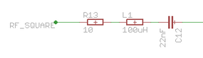
A trained RF designer will probably already noticed the band pass filter in front of the amplifier:
Where the L1 and C12 defines the band pass center frequency and the R13 defines the width of the filter. In the original implementation the values for L1 and C12 was tuned to, more or less, exactly 125 kHz. In this implementation this has been tuned to more closely match 134.2 kHz using the formula:
Source: http://en.wikipedia.org/wiki/LC_circuit

where f0 is the target frequency.

Having this input filter basically means that any signals containing frequencies other than the center frequency are damped through the filter. This comes in handy when it comes to generating the actual frequency signal. An expensive way of generating this input frequency whould be to have a crystal that exactly match the intended frequency. But a much more affordable solution will be to use a frequency output of the MCU that is supposed to decode the signal in the other end anyway. So using a timer on e.g. an AVR XMEGA device to produce a frequency correct "PWM" signal at exactly 134.2 kHz will mean that the only cost to the solution will be to route out another signal from the MCU.

The challenge is that the digital on-off "PWM" signal (square wave signal) will contain much more frequencies than just the main/center frequency. This is due to the nature of rapidly changing signals, i.e. an infinite sharp change in voltage in the time domain, means en infinite wide response in the frequency domain, i.e. the signal contains an infinite amount of frequencies. Think of a lightning bolt, if you listen to the radio, or watch TV you can hear the lightning bolt as a tick or see it as a disturbance on the TV no matter what channel you are tune in on, this is because the lightning bolt is a  very sharp change in the surrounding air voltage, causing it to transmit its signal across all channels and frequencies.  This is quite a big subject in itself so I will not describe more in detail here how this works (for more information see: http://en.wikipedia.org/wiki/Fourier_transform). Long story short, a square wave signal will be dominated by the main/center frequency, but will also contain a considerable amount of 2x the frequency, 3x and so on. So what the band pass filter does is to filer out any other frequencies than the main/center frequency, giving a clean sine signal out as input to the amplifier. That way we know that will will not disturb the neighbors 8'o clock radio news, or your own cellphone signal, or your garage door opener and so on.

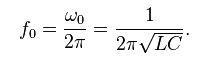
When it comes to the design of the filter, I have already mentioned the L (inductor) and C (capacitors) role, they decide the center frequency of the filter. The R (resistor) on the other hand decide the width of the filter (or band width), i.e. a higher R will cause the filter to accept more frequencies around the center frequency, and keep in mind that the filter is quite sensitive to small changes in R. The reason why we want a certain width of the filter is that using standard components it is often difficult to get exactly the correct frequency you need for your application. So in my circuit I use L = 100uH and C = 22nF which gives a center frequency of 107.302 kHz which is relatively far away from the desired 134.2 kHz, but using the R to increase the bandwidth of the filter means that it will work on 134.2 kHz as well. A small note worth looking into is that inductors could have high internal resistance, which means that the filter might become too wide and start including square parts of the input signal, which is unfortunate. Make sure to use inductors of a certain quality with a small internal resistance. The transmitter will be identical for different types of RFID standards, i.e. ASK (amplitude shift keying), FSK (frequency shift keying), PSK (phase shift keying), and so on.

Receiver

My implementation uses ASK (amplitude shift keying) as it is defined in the ISO11785, since that is the target of the application, to read the ear tags on sheep.

ASK, or amplitude shift keying, means that the digital information is carried in the amplitude of the signal, where keys refer to the actual bit words, i.e. what defines a 1 and 0 in the signal transmission. The radio signal itself is more or less identical to what you see as AM on your car radio, on AM music, voice, etc. are transmitted using changes in the amplitude of the signal, vs. in the change of frequency as it is on a FM radio.


The receiver part consist of an input filter, envelope detector (http://en.wikipedia.org/wiki/Envelope_detector) and operational amplifiers (OPAMP), which amplify and filter the signal further, lastly it uses one OPAMP to digitize the signal.

The clever thing with this design is that the antenna becomes part of the input filer as most RFID antennas are effectively inductors or coils of copper wire. This antenna is then put in series with a capacitor to form a band pass filter as the one for the transmitter where the center frequency is, in my case, 134.2 kHz.

This means that the carrier frequency, 134.2 kHz, will be lead directly to ground, which in turn means that we will have maximum current going through the antenna, which again means increased reading range, and that the carrier frequency has been removed from the input of the envelope detector. This might not make sense, but even though I have already talked about how the information is transmitted in the amplitude of the signal, we are in fact interested in getting rid of as much of the carrier frequency (134.2 kHz) as possible, as the information is in a much lower frequency band than the carrier frequency, called base band (http://en.wikipedia.org/wiki/Baseband). So this means that the information signal is available on what is marked INPUT_SIGNAL in the above drawing, the rest of the signal is lead directly to ground.

Antenna design

For the antenna I picked up some copper wire from http://www.hobbyengineering.com (H04443-01P Enamel Magnet Wire 34 AWG), this works perfectly for winding RFID antennas. I typically use apps like the ElectroDroid to calculate the amount of turns based on the physical size of the antenna and match it with a standard capacitor value, but any other inductor calculator tool will do. The Androide one is just because it is convenient. The results are something like this:
Using the app alone works as a guideline, the finished antenna is close to what you wish, but often not close enough. And it is important to match the antenna and capacitor very well for the system to perform well, any miss-match will typically reduce the reading distance and increase the noise at the receiver end. The above antenna is approximately 2.0 mH, which in my application match exactly with a 680 pF capacitor to form a band pass filter at 134.2 kHz (~116 turns).

To tune the antenna I found that the easiest way was to hook one end of the antenna to a resistor and the other to the capacitor as shown in the schematic below, so that you now have a series network with a resistor, antenna (inductor), capacitor, and ground. Then I hooked a signal generator up to the top most pin of the resistor, and an oscilloscope to the other pin of the resistor:
The signal generator is put in sweep mode around the frequency we are targeting, e.g. 110 kHz to 170 kHz, a long enough time resolution on the oscilloscope will no show a dip of amplitude of the signal at exactly the point where the antenna inductor and capacitor are matched. Often signal generators have an output that will toggle a pin at a certain frequency, this comes in handy here, where this can be used to determine the exact frequency the circuit match. If one set this toggle to happen at the target frequency, e.g. 134.2 kHz and connect the input to another input on the oscilloscope it is easy to see if the current setup matches or not. If it does not match one have to start to either remove or add windings to the antenna. By continuing to add or remove windings until the the signal generator toggle and the lowest point of the amplitude of the output signal are exactly on the same spot one have a perfectly matched antenna.

Envelope detector

After the antenna the signal is fed into an envelope detector, that simply means that the carrier frequency, 134.2 kHz in this case, is filtered out, and you are left the the change in amplitude of the signal only on the positive side.

The signal will swing around zero before entering the diode, where the amplitude will be equally far from zero on the positive side as the negative side. After the diode; the signal is filtered using a series of caps and resistors, the value of these caps and resistors are govern by the bit length, i.e. they have to smooth the signal enough for the carrier frequency, 134.2 kHz, to be filtered away, but fast enough to not filter away the bit information (high-low / low-high) in the amplitude signal. Next the signal is fed through 3 stages of operational amplifiers.

Operational amplifier

The first operational amplifier is in inverting configuration and has a gain of 1MOhm/22kOhm = 46.455 times, and has a low pass filter effect due to the 47pF capacitor. The two diodes are there to reduce the effect of fast changing signals, e.g. a spike due to static discharge. The idea is that if the voltage between the output and input of the opamp is above the threshold of the diode, typically 0.7V, it will be a short between the output and input effectively giving a gain of 1, and not 46. In that way voltage spikes will be damped through the system. I have found that these diodes are not necessary to make the circuit work, but it is always wise to have to possibility to add them if it turns out to be a problem.

The positive side of the opamp is connected to the center voltage, the reason for this is that, at least in my application, negative voltage is not available. Typically operational amplifiers have a positive and negative power-supply, e.g. +12V and -12V, and the operational or working point will then be 0V. In this application the working point of the opamp has been moved upwards to half the supply voltage, that way one do not need the extra negative supply voltage, but of course one will have a smaller operational range of the opamp.

The next opam in the chain is very similar to the first one, and adds additional gain and filter to the signal. In this application I added a pot-meter to be able to control the gain of this second step, but I found that a value of 5kOhms are about correct. This gives a gain of this stage at 200 times.

The total gain in the system is now 200 * 46.455 = 9291 times. So if the system runs on 9V we will have a maximum input on the amplitude of the RF signal to 9V/2 (half the voltage due to the working point of the opamp) = 4.5V/9291 ~ 48mV. That way none of the opamps so far will go into saturation.

The last opamp stage is used a bit differently, here you want the opamp to saturate, either at the low end or at the high end.

If the input signal to this opamp is over the THRESHOLD it will output 9V (or the opamp high supply voltage), if the input signal is below it will output 0V.

The RF amplitude signal has now been demodulated through the envelope detector, filtered and amplified through two stages of operational amplifiers, and at the end digitized using the saturation properties of opamps. The last voltage divider has been added to reduce the voltage down to a level that is safe for the XMEGA MCU (3.3V) that reads the signal.

The next blog post in this series will be on decoding the actual digital signal using an Atmel ATxmega32A4U MCU.

Monday, March 3, 2014

Creating a RFID Reader From Scratch Part 1

For a couple of years now, each fall, I've been attending the ritual of collecting sheep from their  summer pastures in the mountains to get them back to their farm and owners for the winter. The way this works is that people are walking around in the mountain looking for sheep, and when finding them they are herded back to a central collection place. I've been part of the group that stays at the collection place and sort the animals to the correct owner. Currently there are about seven farmers collecting sheep to the same place, and about 1000 - 1400 sheep that is collected, weighted and sorted in the course of two days.

A couple of years ago it became mandatory in Norway to mark each sheep with an electronic ear tag (RFID) that identifies the animal with country, farm and animal number. Being an engineer I came to the conclusion that it must be possible to either get a reader or make a reader for this ear tag myself. This could then speed up the weighing and sorting process by reading the owner of the animal by radio signals instead of manually reading the owner of every sheep. So I started looking around on the internet for an affordable commercial RFID reader, which it is heaps and loads of, but most of them are for 125 kHz or 13.56 MHz, only a few for the 134.2 kHz required to read the animal tags and with a hefty price tag. So I decided to use my RF degree from university and try to implement my own reader.

In the first iteration of the project I started looking for RFID reader modules/IC's, e.g. something like this one from Sparkfun, but for the animal RFID frequency. After looking around and not finding modules that seemed to be a good fit, at least easy to use and implement I decided to have a go at creating a reader from scratch, and really put my RF background to the test.

The principle of a RFID reader is quite simple, you have to generate a radio signal at the correct RF frequency, expose the RFID tag, and then the tag will use the received signal to power itself and generate a radio signal on the same frequency and transmit this back to the reader. A figure for such a system is shown below:


The main challenge in this system is the same as for most radio systems, the receiving signal is very weak. But in a RFID reader system you have an additional factor which you normally try to keep as far away from your "normal" receiver as possible, and that is a strong transmitter in close proximity interfering with the message you are trying to read. This means that constructing the transmitter part (the left part of the figure above) needs careful considerations, but also the receiver needs careful construction to be able to cope with the transmitting signal which is millions of times stronger than the received signal, and yet be capable of decoding the signal.

So the challenge was clear... or was it: build a RFID reader for the 134.2 kHz with an unknown, modulation and data encoding scheme. What I did then was to start looking around the internet for similar projects, I found non on animal RFID, and only a few projects for "normal" RFID, but then I stumbled across this one: https://instruct1.cit.cornell.edu/Courses/ee476/FinalProjects/s2006/cjr37/Website/index.htm, which is a school project where they have implemented a RFID door look system from scratch, and more importantly with discreet components. This meant that the circuit could be tuned to fit my project. However given that the RF modulation would be the same or similar for my animal RFID tags. But it turns out that this project had a very interesting reference: Microchip has posted an application note on RFID readers from discreet components: http://ww1.microchip.com/downloads/en/DeviceDoc/51115F.pdf. And suddenly there was a hope for my project after all.

The next hurdle was to find some more information on the exact implementation of the ear tag itself, and it turns out that there is an ISO standard that defines the animal RFID: ISO11784 and ISO11785 (http://en.wikipedia.org/wiki/ISO_11784_%26_11785). The standard operates with two (or three) different protocols one is the full duplex (FDX & FDX-B) and the other half duplex (HDX). The difference is that on the FDX protocol the RFID tag sends data at the same time as the transmitter sends its RF energy to power the internal logic of the tag, the HDX type you burst the tag with power for a given time and then you turn off the transmitter and wait for a reply. There are pros and cons with both protocols, that I will not cover in details in this article, but the most obvious once are that in the HDX system the readers receiver can be simpler because the readers transmitter is off and will not interfere with the signal of the message from the tag, while in the FDX system the transmitter must remain on while the entire communication is flowing, making it difficult for the reader receiver to "hear" the information coming from the RFID tag. But for the FDX system the tag itself is simpler, in the HDX tag you would need a capacitor to store the energy needed to transmit the signal back to the reader, and capacitors takes up space and are expensive. The easiest comparison that I can think of is that you can picture that you need to shout a given amount of sound to your friend for him or she can be able to reply. In the HDX system you will be shouting to your friend for a certain amount of time, before you shut up and your friend is able to whisper his or hers message back to you. In the FDX system you would need to shout the entire time while your friend is trying to whisper his or hers message back to you, obviously making the communication very difficult.

Now I at least had a few clues to go after, so I  began some initial testing. I had a few of the ear tags to test on so I started to expose them with RF energy using a simple signal generator and a coiled up insulated copper wire to act as an antenna. In the other end of the coil i put a resistor to ground and an oscilloscope across the resistor. This allowed me to clearly see the 134.2 kHz sine wave plus a bunch of noise. Moving the ear tag closer and further from the "antenna" (insulated copper wire coil) I saw a distinct change is the noise pattern, so I started searching for the HDX "signatures", i.e. 124.2 kHz and 134.2 kHz after turning off the "transmitter", I was kind of hoping that it was a HDX system and not a FDX system having the idea that the HDX would be easier to implement when I came to that point. But I saw no signs of any RF activity after turning off the transmitter, only when the transmitter was on, and in the area of the FDX tags. So I started working on the hypothesis that the system was either FDX or FDX-B with ASK (amplitude shift keying) and DBP differential bi-phase keying (more on this in later parts of the RFID series).

I started working on implementing the ASK reader described in chapter 4 in the Microchip PDF. With discreet components on a prototype PCB. In the next part in this series of articles on the RFID design I will show what modifications needed to be done on both the transmitter part and the receiver part to make it work with a different frequency. Thank you for reading so far, and keep tuned for the next parts in the series, where I will look in detail on the actual implementation and suggest a complete solution using SMD components and my reflow oven (will make another post on the reflow oven) to produce the result below:


Saturday, January 18, 2014

Creating an Atmel Xplained Pro to Arduino Adapter

It's always interesting the try to create something based on someone's specifications. This often because there is always a small element of doubt if the specification is correct, typos could have sneaked in, new revisions of the spec may exist and so on. But it's a very satisfying feeling when you get the design back from the fab solder it up and it actually fits.


Arduino Xplained Pro
 This Xplained Pro to Arduino adapter project was absolutely one of these projects. I've never made a Atmel Xplained Pro extension before, so that was the first obstacle, finding the specification to the header location and pin functions. After some poking around on Atmel.com I found the specs on this page: https://gallery.atmel.com/Partner. Next I had to tackle the Arduino specification, this was a much easier as there are loads of available Arduino projects for Eagle out there, and Arduino post the Eagle files themselves so grabbing the specifications from there was easy.
SAM D20 Xplained Pro with Arduino Xplained Pro


The Arduino specification I moved into a part in my Eagle library, so now for future Arduino shields or MCU boards I can simply add the Arduino board part, which will add the board outline and all connectors.

One thing that was a bit difficult when making the adapter was to deside which pins on the Xplained Pro header should be connected to which pin on the Arduino. And also the issue with the Xplained Pro header did not contain enough signals to fill all the signals on the Arduino. Especially the analog pins as the Xplained Pro header only specifies two analog pins per header, so the signal A2-A5 are not connected. Other than that most functions are kept, like the UART/USART, SPI, I2C are fully operational. I used the Arduino Ethernet shield as guide for which pins could be omitted without any impact on the function on that particular shield, as one of the main driving forces behind this project was to create an Atmel SAM D20 web server.

I ended up having to omit signals RST, VIN, A2-A5, AREF, 8 and 9. So all in all most of the Arduino functions are kept. The nice thing with this adapter is that it fits to the entire range of Atmel Xplained Pro boards, and opens up for using Arduino shields with the Atmel MCU's which is not officially supported by their own Arduino MCU board.

When the design was done I sent the project off to the fab, OSH Park, and waited patiently for my first adapter PCB project. I got the PCB back and things looked promising, so I sent off a few pictures to one of the people waiting for the result and I got the very fitting comment: "Now populate that sucker and let's see if it catches fire." And luckily no fires was observed once assembled and connected to the Xplained Pro board. And within a few days the Arduino Ethernet shield was up an running on the SAM D20 using Arduino C++ code.

The finished design with Eagle project, schematic, board and gerber files are available here: https://github.com/ivarho/ArduinoXplainedPro.

Or one could go directly to the OSH Park and order the design: http://www.oshpark.com/shared_projects/X7ivSLb0.

For the Eagle library: https://github.com/ivarho/eagle_library


Edit:
I found an issue with version 1.0 where the SDA and SCL pins was interchanged, this has now been fixed in the version 1.1 of the board, the repos (both library and project) and the OSHPark shared project link has been updated.